hybrid 2D/3D perovskite structures for photovoltaics with improved stability — interface engineering with nanoparticles (carbon and perovskite nanodots, MXene nanoflakes) for defect passivation, in-operando X ray scattering (GIWAXS), photoluminiscence, galvanostatic electrochemical impedance spectroscopy (GEIS) and J-V curve studies for performance optimization and stability enhancement
(anode-free) lithium batteries with solid-state electrolyte — development of simultaneous in-operando GIWAXS and GEIS monitoring of spatio-temporal evolution of stresses and interfaces during battery cycling for tracking the migration of Li ions and the study of the effect of the accompanying phenoma on the battery perfomance (at synchrotron and in laboratory)
self assembly effects of low-dimensional materials at the liquid-air interface and formation of supported 2D and 3D assemblies by Langmuir–Schaefer method (metal and metal oxide nanoparticles, carbon and perovskite nanodots, nanoflakes of 2D materials — graphene, transition metal dichalcogenides, MXenes)
application of 2D materials to advanced theranostics — development and in-vitro testing of 2D bioconjugated functionalized nanoplatforms (graphene and MoS2 nanoflakes, MoOx nanodots) for targeted anti-cancer drug delivery and/or contrast imaging utilizing photothermal, photodynamic or magnetic hyperthermia effects
electronic structure, defects and charge transfer in organic semiconductors and electrolytes studied by deep-level transient spectroscopy (DLTS) in time domain, energy-resolved electrochemical impedance spectroscopy (ER-EIS) and electrochemical methods (steady-state and cyclic voltammetry, voltcoulometry, chronocoulometry)
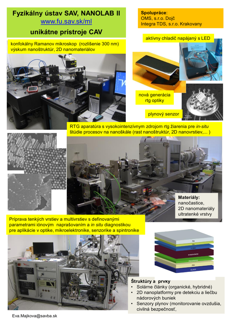
functional thin film structures for (opto)electronics prepared by ion beam sputtering with in-situ monitoring by ellipsometry and small-angle X-ray scattering, their complex characterization by scanning probe, optical, electrical and X-ray methods
self assembly effects of low-dimensional materials at the liquid-air interface (metal and metal oxide nanoparticles, carbon and perovskite nanodots, nanoflakes of 2D materials) and formation of their supported 2D and 3D assemblies by Langmuir-Schaefer method studied in real time by in-situ grazing incidence small- and wide-angle X-ray scattering (GISAXS, GIWAXS) techniques at ambient and non-ambient conditions
diffractive X-ray optics for X-ray metrology and X-ray bioimaging — computer design and testing of V shaped channel cut monochromators for the X ray beam compression and expansion, complex characterization of the diffractive surfaces for implementation of single-point diamond turning and flying cutting technologies in the X-ray optics
development of dedicated laboratory equipments for diagnostics of nanostructures — lab-GISAXS for in-situ small-angle X-ray scattering experiments with 25 ms time resolution, fast null ellipsometer with 5 ms time resolution, magneto-optical Kerr microscope with autobalance detection scheme and spatial resolution 500 nm, scanning charge transient microscope for probing deep levels in organic and inorganic semiconductors in isothermal regime with resolution of the transient charge of 600 eV, setup for the energy-resolved electrochemical impedance spectroscopy allowing a complete DOS mapping between HOMO and LUMO of organic semiconductors
custom-designed dual ion beam sputtering machine (Bestec) with in-situ ellipsometry and in-situ GISAXS monitoring, base pressure 2 × 10⁻⁸ mbar, working pressure 4 × 10⁻⁴ mbar
Laboratory of photovoltaics
glove box (Jacomex) interlocked with vacuum chambers (Bestec) for deposition of metallic and organic layers
Kelvin probe for surface potential measurements
I-V tracer with solar simulator SUN 2000 (Abet Technologies)
quantum efficiency measurements (Rera Solutions)
laminar box with controlled humidity
Laboratory of battery research
MBraun glove box interlocked with X-ray setup with IμS Cu microfocus X-ray source (Incoatec) and 2D detector Pilatus 200K (Dectris)
MBraun glove box interlocked with Nanostar X-ray setup (Bruker) with IμS Cu microfocus X-ray source (Incoatec) and 2D detector Eiger 2R Si 500K (Dectris)
X-ray setup with IμS Ag microfocus X-ray source (Incoatec) and 2D detector Eiger 2R CdTe 500K (Dectris)
Laboratory of laser beam technologies
high-power 1.4 kW 355 nm UV laser TruMark 6330 (Trumph) with 7 ns pulses, pulse repetition frequency 1–120 kHz, min. focal diameter 16 μm, max. size of irradiation field 170 × 170 mm2
Preparatory chemical and thermal treatment laboratory
3 fume hoods, analytical microbalances, ultrasonic, rotational and magnetic stirrers, centrifuges up to 60k rpm, reaction chambers for ozonolysis and UV photolysis, hot plates, vacuum furnace for rapid thermal annealing up to 1000 °C, high-temperature furnace and other auxiliary instrumentation
X-ray laboratory
modular setup for small-angle X-ray scattering (own development) with microfocus 30 W source (Incoatec) and 2D detector Pilatus 100K (Dectris)
Nanostar setup (Bruker) for small- and wide-angle X-ray scattering (SAXS, WAXS) with 2D detectors Pilatus 300K (Dectris) and Vantec 2000 (Bruker) and 250 W Ga liquid metal-jet anode microfocus source, primary beam flux 109 photons/s (Excillum)
D8 Discover SSS setup (Bruker) equipped with 18 kW rotating anode generator (Rigaku) and Goebel parallel beam optics for X-ray diffraction and X-ray reflectometry, primary beam flux 109 photons/s
multifunctional adaptive UHV setup with temperature control from LN2 to > 1000 K (Prevac) for X-ray studies under non-ambient conditions with Nanostar IμS Cu microfocus X-ray source (Incoatec), Vantec 2000 detector and imaging plate for (GI)SAXS and (GI)WAXS
Laboratory of optical and spectroscopic techniques
UV-VIS-NIR spectrophotometer, spectral range 200–2200 nm (Shimadzu)
optical 3D microscope 500× with large working distance (Hitachi)
imaging ellipsometer with spatial resolution 10 × 10 μm (Accurion)
spectroscopic ellipsometer, spectral range 350–1000 nm (Woolam)
spectroscopic ellipsometer, spectral range 260–1000 nm (Sentech)
fast tracking ellipsometer with 5 ms temporal resolution (own development)
scattering-type scanning near-field optical microscope (s-SNOM) with a nano-FTIR module with a wavelength range 660–5000 cm-1, lateral and vertical resolutions down to 20 nm (Neaspec)
confocal microscope LSM 900 for advanced bioimaging and surface topography with a resolution down to 90 nm (Zeiss)
3D optical profilometer ContourX-500 with a 5MP camera with a 1200 × 1000 measurement array and enhanced stitching capabilities (Bruker)
photoluminescence spectrometer FLS1000 for steady state and time-resolved photoluminescence measurements from the ultraviolet to the mid-infrared spectral range and the lifetimes from picoseconds to seconds (Edinburgh Instruments)
Laboratory of scanning probe techniques
metrologic atomic force microscope Dimension Edge (BrukerNano)
multimode atomic force microscope Multimode 8 (BrukerNano)
stylus profilometer Dektak 150 (BrukerNano)
long-trace profiler (Bruker)
atomic force microscope JPK NanoWizard for bioAFM with atomic resolution, scan range up to 100 micrometers and scan rate up to 150 lines/s (Bruker)
Laboratory of electrical and electro-chemical measurements
cyclic voltammetry and coulommetry
deep-level transient charge spectroscopy
electrochemical impedance spectroscopy
chamber with mass-flow controller for resistivity measurements in gases